Meaning of SMT
Surface Mount Technology (SMT): This is the most common meaning of SMT in electronics manufacturing. It refers to the technology of mounting pinless or short-pin electronic components directly onto the surface of a printed circuit board (PCB). This technology has the advantages of high productivity, high automation, small size, light weight and high reliability, and is widely used in the manufacturing of modern electronic products.
Differentiation of SMT solutions for different application scenarios
The requirements for SMT vary greatly from one application scenario to another, and a single standardized process can no longer meet the needs of high reliability, special packaging, and extreme environmental adaptation. With the increasing penetration of electronic products into medical, automotive, industrial control, consumer electronics and other fields, different industries have different requirements for SMT assembly standards, reliability, cost control, product consistency and other requirements.
Highly Reliable SMT Means in Medical Electronics
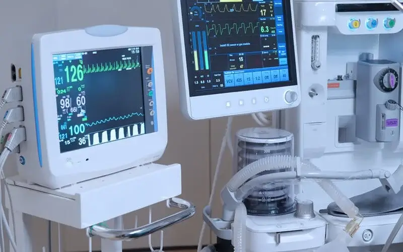
For example, in the field of medical electronics, the reliability requirements of the SMT process are nearly extreme. Since the products are often used in critical applications such as life support systems and diagnostic instruments, the control of solder quality, component consistency and board cleanliness is very stringent, often even exceeding that of industrially controlled products. In practice, parameters such as solder paste printing, reflow temperature profiles and component ESD protection must be specifically defined. In addition, due to the small batch sizes and complex designs of most medical products, SMT manufacturers need precise process control capabilities and must be equipped with MES systems to ensure traceability throughout the manufacturing process in order to comply with regulations such as ISO 13485 or FDA standards.

Highly Reliable SMT Tools for Automotive Electronics
In contrast, automotive electronics presents more stringent requirements from another dimension. Automotive electronic control systems are often deployed in environments with extreme temperature variations, strong vibrations and high humidity, which require SMT processes with stronger solder joints and higher environmental resilience. Common optimization strategies for such projects include the use of thick copper PCBs to enhance thermal conductivity, high-reliability solders to resist thermal cycling fatigue, and triple-proof coatings after assembly to further enhance corrosion resistance. In addition, automotive electronics make extensive use of aging and vibration tests, which require SMT manufacturers to have a systematic and automated quality control system. Therefore, partners in the automotive field not only need to have the necessary equipment capabilities, but also need to obtain IATF 16949 and other automotive quality system certification.

Flexibility and stability of SMT process for industrial electronics products
Compared to the first two categories, industrial control electronics focuses more on the balance between process flexibility and product stability. These products are usually used in long-term operation of industrial equipment, emphasizing the continuous supply of circuit boards and long-term maintenance. As a result, they tend to adopt more conservative component selection and more lenient soldering standards. For example, in some high-reliability industrial controller projects, we often encounter customers who require a mix of SMT and THT (through-hole technology) assemblies, or who need to solder high-power and irregularly shaped components, which poses a challenge to flexible line switching and customized fixturing capabilities. In addition, industrial products have long life cycles and less frequent BOM changes, but the risk of production interruption due to errors is much higher than in consumer electronics. Therefore, contract manufacturers need well-established NPI (New Product Introduction) and ECN (Engineering Change Notification) processes to ensure a smooth transition between process validation and mass production.

Cost Effectiveness of SMT for Consumer Electronics
In contrast, consumer electronics are more focused on cost control and economies of scale in their SMT requirements. These products have fast iteration speeds, short life cycles, and the market is highly price-sensitive. Therefore, the core competitiveness of SMT outsourcing often lies not in the complexity of the process, but in the possession of high-speed and efficient production line resources. For example, the high-density placement of ultra-small components such as 0201, 01005, etc. requires the mounter to have extremely high positioning accuracy and visual recognition capabilities, while the dual-track production line and automatic loading and unloading systems become the key to scale production efficiency. In addition, because consumers attach great importance to the product’s “first impression”, consumer electronics on the circuit board appearance, weld uniformity, logo clarity and other requirements are also higher. This requires that the SMT process should not only be efficient, but also aesthetically pleasing. Routine inspection processes such as AOI and SPI must cover the entire workflow, rather than relying on sampling or localized inspections.

From the above comparison, it can be seen that the nature of the SMT process is similar, but in different scenarios, there are significant differences in its technical realization. Medical electronics focuses on high reliability and fine traceability, automotive electronics emphasizes environmental resistance and structural strength, industrial electronics focuses on process customization and long-term stability, while consumer electronics pursues production efficiency and cost control. A truly outstanding SMT foundry must be flexible enough to switch between these different needs, execute with precision, and provide customers with integrated process support from product design, prototype validation to mass production assembly.
What does DFM mean for SMT?
In modern electronics manufacturing, SMT (Surface Mount Technology) and DFM (Design for Manufacturability) are two highly interrelated processes; SMT is responsible for efficiently and accurately soldering electronic components to PCBs (Printed Circuit Boards) using automated equipment, while DFM anticipates and mitigates potential manufacturing issues during the design phase to improve the overall manufacturability of a product. The common goal of both is to improve production yields, reduce manufacturing costs, and accelerate the cycle time from design to mass production.
First, during the component selection and package design phase, DFM should interface with SMT process capabilities, prioritize standard package types, and ensure that the package library meets IPC design standards. For high-density assembly boards, it is recommended to avoid the use of too small packages (e.g., 01005) or packages with narrow process windows to reduce assembly and soldering difficulties. In addition, in terms of pad design, DFM should recommend appropriate pad size, shape and spacing according to SMT process characteristics to ensure the accuracy of solder paste printing and component placement.
Secondly, during PCB wiring and structure design, DFM needs to fully consider the SMT production process. Cabling should avoid placing over-holes, alignments or copper foil cuts in the assembly area, as these factors can affect the thermal balance during reflow and may lead to cold soldering or warpage. For double-sided mounted boards, the DFM must also evaluate the reflow process sequence and the effect of thermal stress on components to optimize the stacking structure and thermal layout.
In terms of stencil design and solder paste printing, controlling the amount of solder is critical to the SMT process, and the DFM can provide recommendations for stencil openings, shapes and thicknesses based on component size and pad structure. For QFN or BGA components, stepped stencils or trimmed openings are recommended to avoid bridges and voids. These design recommendations usually come from feedback based on SMT production line experience, so the DFM should establish a close communication mechanism with the SMT team.
In addition, panel design and component placement orientation are important aspects of collaboration. DFMs should consider paneling methods (e.g., V-Cut or pole-and-ear routing), fixture space, and placement paths during the design phase to better fit the SMT production workflow. Standardizing component placement orientation not only improves placement speed, but also reduces the time wasted by frequent material changes at the placement machine.
In order to better realize the integration of design and manufacturing, GLinkPCB can automatically detect potential manufacturing problems at the early stage of design, help engineers optimize the PCB structure, improve mass production yields, and accelerate the cycle time from design to delivery.
About GLinkPCB
In project development, time is of the essence – and GLinkPCB can meet your needs. We provide you with a one-stop solution for PCB manufacturing and assembly, turning your design into reality quickly and precisely. From high-quality bare boards to state-of-the-art PCB assembly, GlinkPCB can handle prototyping and mass production. Partner with us to streamline your supply chain and accelerate your projects with reliable and trustworthy PCB solutions.


